- 您现在的位置:买卖IC网 > Sheet目录1997 > ICS843002AKI-41LF (IDT, Integrated Device Technology Inc)IC SYNTHESIZER LVPECL 32-VFQFPN
ICS843002I-41
700MHZ, FEMTOCLOCK VCXO BASED SONET/SDH JITTER ATTENUATOR
IDT / ICS VCXO BASED SONET/SDH JITTER ATTENUATOR
7
ICS843002AKI-41 REV. B
APRIL 7, 2009
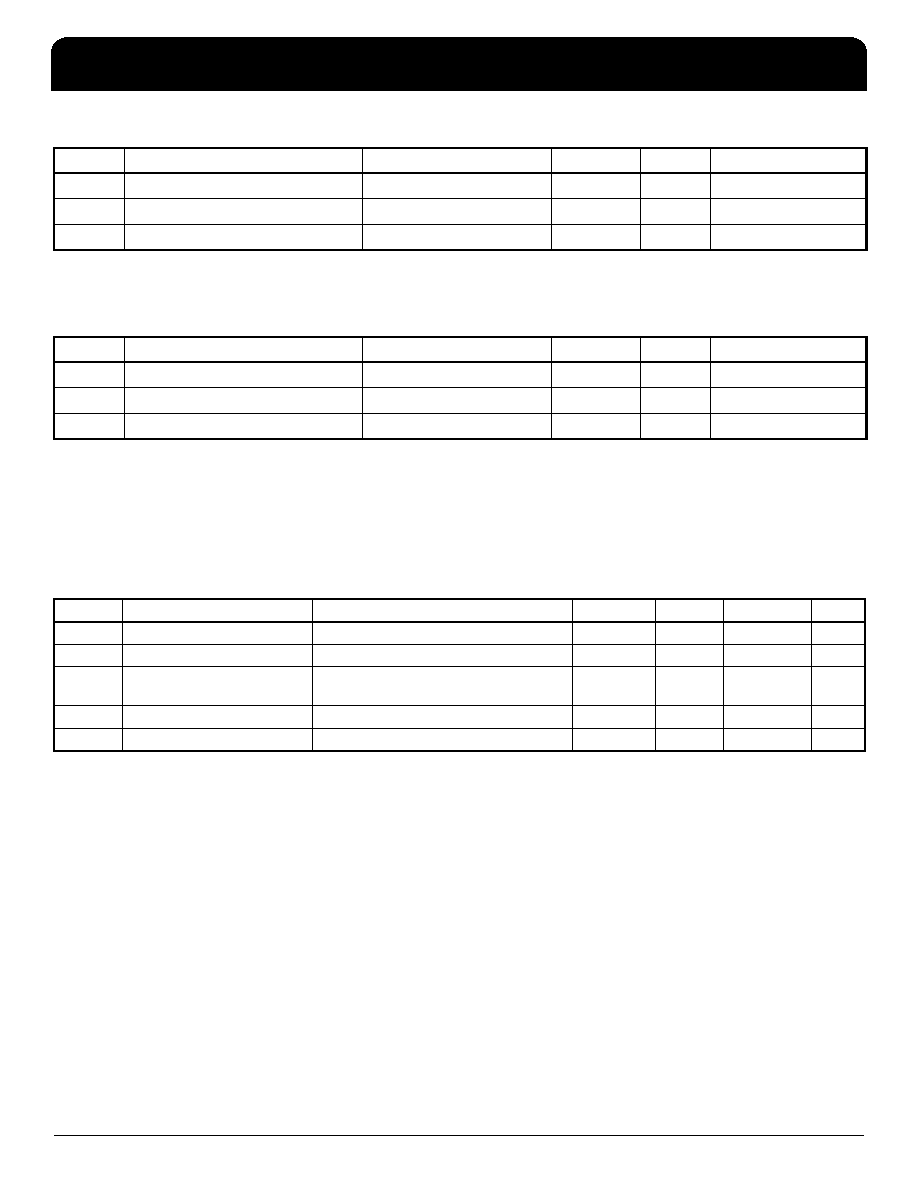
Table 4D. LVPECL DC Characteristics, VCC = VCCO_LVPECL = 3.3V±5%, VEE = 0V, TA = -40°C to 85°C
NOTE 1: Outputs terminated with 50
Ω to V
CCO_LVPECL – 2V. See Parameter Measurement Information section, Output Load Test Circuit
diagram.
Table 4E. LVPECL DC Characteristics, VCC = 3.3V±5%, VCCO_LVPECL = 2.5V±5%, VEE = 0V, TA = -40°C to 85°C
NOTE 1: Outputs terminated with 50
Ω to V
CCO_LVPECL – 2V. See Parameter Measurement Information section, Output Load
Test Circuit diagram.
AC Electrical Characteristics
Table 5. AC Characteristics, VCC = 3.3V±5%, VCCO_LVCMOS = VCCO_LVPECL = 3.3V±5% or 2.5V±5%, VEE = 0V,
TA = -40°C to 85°C
See Parameter Measurement Information section.
NOTE: Electrical parameters are guaranteed over the specified ambient operating temperature range, which is established when the
device is mounted in a test socket with maintained transverse airflow greater than 500 lfpm. The device will meet specifications after
thermal equilibrium has been reached under these conditions.
NOTE 1: Defined as skew between outputs at the same supply voltage, same frequency, and with equal load conditions.
Measured at the output differential cross points.
NOTE 2: This parameter is defined in accordance with JEDEC Standard 65.
NOTE 3: Please refer to the Phase Noise plots.
Symbol
Parameter
Test Conditions
Minimum
Typical
Maximum
Units
VOH
Output High Voltage; NOTE 1
VCCO – 1.4
VCCO – 0.9
V
VOL
Output Low Voltage; NOTE 1
VCCO – 2.0
VCCO – 1.7
V
VSWING
Peak-to-Peak Output Voltage Swing
0.6
1.0
V
Symbol
Parameter
Test Conditions
Minimum
Typical
Maximum
Units
VOH
Output High Voltage; NOTE 1
VCCO – 1.4
VCCO – 0.9
V
VOL
Output Low Voltage; NOTE 1
VCCO – 2.0
VCCO – 1.5
V
VSWING
Peak-to-Peak Output Voltage Swing
0.4
1.0
V
Symbol
Parameter
Test Conditions
Minimum
Typical
Maximum
Units
fOUT
Output Frequency
19.44
700
MHz
tsk(o)
Output Skew; NOTE 1, 2
150
ps
tjit()
RMS Phase Jitter (Random);
NOTE 3
155.52MHz,
Integration Range: 12kHz – 20MHz
0.81
ps
tR / tF
Output Rise/Fall Time
20% to 80%
100
800
ps
odc
Output Duty Cycle
45
55
%
发布紧急采购,3分钟左右您将得到回复。
相关PDF资料
ICS843004AG-02LF
IC SYNTHESIZER LVPECL 24-TSSOP
ICS843004AGI-04LF
IC SYNTHESIZER LVPECL 24-TSSOP
ICS843021AGLFT
IC CLK GENERATOR LVPECL 8-TSSOP
ICS843022AGLF
IC CLK GENERATOR LVPECL 8-TSSOP
ICS843023AGLF
IC CLK GENERATOR LVPECL 8-TSSOP
ICS843031AG-01LF
IC CLK GENERATOR LVPECL 8-TSSOP
ICS843081AGI-01LF
IC CLK MULTIPLIER LVPECL 8-TSSOP
ICS8430AYI-61LF
IC SYNTHESIZER LVPECL 32-LQFP
相关代理商/技术参数
ICS843002AKI-41LFT
功能描述:IC SYNTHESIZER LVPECL 32-VFQFPN RoHS:是 类别:集成电路 (IC) >> 时钟/计时 - 时钟发生器,PLL,频率合成器 系列:HiPerClockS™, FemtoClock™ 标准包装:27 系列:Precision Edge® 类型:频率合成器 PLL:是 输入:PECL,晶体 输出:PECL 电路数:1 比率 - 输入:输出:1:1 差分 - 输入:输出:无/是 频率 - 最大:800MHz 除法器/乘法器:是/无 电源电压:3.135 V ~ 5.25 V 工作温度:0°C ~ 85°C 安装类型:表面贴装 封装/外壳:28-SOIC(0.295",7.50mm 宽) 供应商设备封装:28-SOIC 包装:管件
ICS843002AKI-41T
制造商:Integrated Device Technology Inc 功能描述:IC SYNTHESIZER LVPECL 32VFQFN
ICS843002AKI-72LF
功能描述:IC SYNTHESIZER LVPECL 32-VFQFPN RoHS:是 类别:集成电路 (IC) >> 时钟/计时 - 时钟发生器,PLL,频率合成器 系列:HiPerClockS™, FemtoClock™ 标准包装:27 系列:Precision Edge® 类型:频率合成器 PLL:是 输入:PECL,晶体 输出:PECL 电路数:1 比率 - 输入:输出:1:1 差分 - 输入:输出:无/是 频率 - 最大:800MHz 除法器/乘法器:是/无 电源电压:3.135 V ~ 5.25 V 工作温度:0°C ~ 85°C 安装类型:表面贴装 封装/外壳:28-SOIC(0.295",7.50mm 宽) 供应商设备封装:28-SOIC 包装:管件
ICS843002AKI-72LFT
功能描述:IC SYNTHESIZER LVPECL 32-VFQFPN RoHS:是 类别:集成电路 (IC) >> 时钟/计时 - 时钟发生器,PLL,频率合成器 系列:HiPerClockS™, FemtoClock™ 标准包装:27 系列:Precision Edge® 类型:频率合成器 PLL:是 输入:PECL,晶体 输出:PECL 电路数:1 比率 - 输入:输出:1:1 差分 - 输入:输出:无/是 频率 - 最大:800MHz 除法器/乘法器:是/无 电源电压:3.135 V ~ 5.25 V 工作温度:0°C ~ 85°C 安装类型:表面贴装 封装/外壳:28-SOIC(0.295",7.50mm 宽) 供应商设备封装:28-SOIC 包装:管件
ICS843002ALF
制造商:ICS 制造商全称:ICS 功能描述:FEMTOCLOCKS⑩ CRYSTAL-TO-3.3V LVPECL FREQUENCY SYNTHESIZER
ICS843002BY-31LF
功能描述:IC SYNTHESIZER LVPECL 64-TQFP RoHS:是 类别:集成电路 (IC) >> 时钟/计时 - 时钟发生器,PLL,频率合成器 系列:HiPerClockS™, FemtoClock™ 标准包装:27 系列:Precision Edge® 类型:频率合成器 PLL:是 输入:PECL,晶体 输出:PECL 电路数:1 比率 - 输入:输出:1:1 差分 - 输入:输出:无/是 频率 - 最大:800MHz 除法器/乘法器:是/无 电源电压:3.135 V ~ 5.25 V 工作温度:0°C ~ 85°C 安装类型:表面贴装 封装/外壳:28-SOIC(0.295",7.50mm 宽) 供应商设备封装:28-SOIC 包装:管件
ICS843002BY-31LFT
功能描述:IC SYNTHESIZER LVPECL 64-TQFP RoHS:是 类别:集成电路 (IC) >> 时钟/计时 - 时钟发生器,PLL,频率合成器 系列:HiPerClockS™, FemtoClock™ 标准包装:27 系列:Precision Edge® 类型:频率合成器 PLL:是 输入:PECL,晶体 输出:PECL 电路数:1 比率 - 输入:输出:1:1 差分 - 输入:输出:无/是 频率 - 最大:800MHz 除法器/乘法器:是/无 电源电压:3.135 V ~ 5.25 V 工作温度:0°C ~ 85°C 安装类型:表面贴装 封装/外壳:28-SOIC(0.295",7.50mm 宽) 供应商设备封装:28-SOIC 包装:管件
ICS843002CY31
制造商:ICS 制造商全称:ICS 功能描述:700MHZ FEMTOCLOCKS? VCXO BASED FREQUENCY TRANSLATOR AND JITTER ATTENUATOR